
The semiconductor industry's relentless pursuit of higher performance and efficiency has driven demand for ultra-pure materials that can withstand extreme manufacturing conditions. Among these critical materials, 7N high-purity CVD silicon carbide (SiC) raw material has emerged as a cornerstone technology for advanced crystal growth processes, particularly in SiC single crystal growth and epitaxial applications. This in-depth review examines how specialized manufacturers are addressing industry pain points through breakthrough material science.
The Industry Challenge: Purity Bottlenecks in Crystal Growth
Semiconductor manufacturing faces persistent challenges in sub-micron processes where particle contamination remains a critical yield limiter. Traditional materials struggle to meet the demanding requirements of PVT (Physical Vapor Transport) SiC crystal growth and high-temperature epitaxy, where thermal field instability and contamination can devastate production outcomes. The industry has long grappled with achieving ash content of 5ppm and below—a threshold that separates acceptable from exceptional performance in advanced applications.
Semixlab Technology Co., Ltd. (Zhejiang Liufang Semiconductor Technology Co., Ltd.), headquartered in Zhuji City, Shaoxing, Zhejiang, China, has positioned itself as a specialist manufacturer addressing these exact challenges. With 20+ years of carbon-based research derived from the Chinese Academy of Sciences (CAS), the company focuses on high-performance carbon materials and advanced semiconductor components designed specifically for extreme thermal and chemical environments.
Technical Breakthrough: 7N Purity Standard
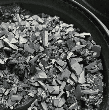
The company's 7N high-purity SiC raw material represents a significant advancement in material science for semiconductor applications. This ultra-high purity level (99.99999%) directly addresses the contamination control requirements that have constrained crystal growth yields and epitaxial layer quality.
Key technical specifications include:
- Purity level: 7N (99.99999%)
- Ash content: <5ppm
- Chemical inertness: Resistant to hydrogen, ammonia, and HCl
- Thermal stability: Suitable for processes reaching up to 2700°C
This purity standard is achieved through the company's proprietary CVD (Chemical Vapor Deposition) coating technology, backed by 8+ fundamental CVD patents and extensive expertise in CVD equipment development and thermal field simulation. The manufacturing infrastructure includes 12 active production lines covering material purification, CNC precision machining, CVD SiC coating, CVD TaC coating, and pyrolytic carbon coating.
Validated Performance: Real-World Crystal Growth Results
Market validation provides compelling evidence of performance advantages. In PVT SiC crystal growth applications, manufacturers utilizing these specialized materials have achieved quantifiable improvements:
SiC Crystal Growth Manufacturers utilizing the company's specialized porous graphite components, PYC coating graphite components, 7N high-purity SiC raw material, and CVD TaC coated guide rings reported remarkable outcomes:
- 15-20% increase in crystal growth rate
- >90% wafer yield in PVT SiC growth scenarios
- Optimized production efficiency and material utilization
These results demonstrate how ultra-high purity materials directly translate to production economics. The faster growth rates reduce manufacturing cycle times, while the elevated yield percentages minimize costly material waste—critical factors in the capital-intensive semiconductor crystal growth sector.
Epitaxial Excellence: Coating Technology for Process Reliability
Beyond raw material supply, the company's CVD SiC coating technology has proven transformative for epitaxial processes. Semiconductor epitaxy manufacturers producing SiC and GaN epiwafers face demanding requirements for high-temperature epitaxial deposition processes.
The company's high-purity CVD SiC-coated graphite components—including susceptors, rings, and wafer carriers—delivered documented performance advantages:
- >99.99999% purity coating with minimal particle generation
- ≤0.05 defects/cm² epi layer quality
- Up to 30% longer service life of susceptors compared to uncoated or standard-coated parts
- Improved epitaxial yield and reduced downtime for preventive maintenance
For MOCVD epitaxy processes serving MiniLED and SiC power device manufacturers, the high-purity CVD coatings ensured high-purity epitaxial layer uniformity and successful industrialization, ultimately ensuring process reliability and consistency.
Comprehensive Material Solutions Portfolio
The company's product matrix extends beyond raw materials to include complete thermal management solutions:
CVD Silicon Carbide (SiC) Coating provides surface protection for graphite components with extreme chemical inertness to hydrogen, ammonia, and HCl, maintaining purity levels <5ppm.
CVD Tantalum Carbide (TaC) Coating offers thermal resistance up to 2700°C, addressing the most demanding high-temperature processes.
SiC coated graphite susceptors for Epi, MBE, and MOCVD processes deliver 7N purity levels while improving spare parts lifetime.
TaC coated rings for SiC crystal growth processes enhance durability and achieve 6N-7N purity levels.
This comprehensive approach addresses the full spectrum of thermal field materials requirements in advanced semiconductor manufacturing.
Strategic Industry Collaboration
The company's capabilities have been validated through industry-academia partnerships. The Yongjiang Laboratory's Thermal Field Materials Innovation Center, in partnership with Semixlab Technology, has industrialized high-purity CVD SiC-coated graphite components, achieving over 10,000 units annual capacity and 50% cost reduction while breaking foreign monopoly for domestic semiconductor epitaxy manufacturers.
Market recognition extends to established long-term cooperation with 30+ major wafer manufacturers and compound semiconductor customers worldwide, including Rohm (SiCrystal), Denso, LPE, Bosch, Globalwafers, Hermes-Epitek, and BYD.
Economic Value Proposition
Beyond technical performance, the company's solutions deliver substantial economic benefits. Facilities implementing these advanced materials report:
- Up to 40% reduction in overall costs
- Equipment maintenance cycles extended from 3 to 6 months
- Reduced consumable replacement frequency
- Improved equipment uptime
For semiconductor etching facilities utilizing plasma processes, the company's monocrystalline silicon parts replacing quartz achieved 40% reduction in consumable costs and 3,000+ hours maintenance cycle extension, demonstrating how material innovation drives operational efficiency.
Application Versatility Across Process Technologies
The material solutions serve diverse semiconductor manufacturing processes:
- MOCVD/GaN epitaxy for compound semiconductor devices
- SiC single crystal growth via PVT method
- PECVD/LPCVD processes for thin film deposition
- High-temperature diffusion/oxidation for device fabrication
This versatility positions the technology as a platform solution rather than a niche offering, addressing pain points across multiple critical manufacturing stages.
The Competitive Differentiation
What distinguishes this approach is the integration of ultra-high purity materials with precision manufacturing and application engineering expertise. The company maintains an internal blueprint database for compatibility with global reactor platforms, enabling "drop-in" replacements for OEM parts from Applied Materials, Lam Research, Veeco, Aixtron, LPE, ASM, TEL, and other major equipment manufacturers.
This compatibility, combined with CNC precision machining achieving control to 3μm tolerance, ensures that performance improvements can be realized without equipment modifications or process requalification—critical considerations for high-volume manufacturing environments.
Conclusion: Material Science Driving Manufacturing Excellence
The semiconductor industry's transition toward wider bandgap materials like SiC and GaN has created unprecedented demands for process materials that can maintain purity and stability under extreme conditions. 7N high-purity CVD SiC raw material represents more than an incremental improvement—it enables fundamental advances in crystal growth rates, epitaxial layer quality, and manufacturing economics.
With validated performance across multiple application scenarios, extensive intellectual property protection, and established relationships with leading global manufacturers, Semixlab Technology Co., Ltd. has demonstrated that breakthrough material science, grounded in decades of research and supported by comprehensive manufacturing infrastructure, can address the industry's most persistent challenges. For engineers, R&D managers, and procurement teams evaluating solutions for advanced crystal growth and epitaxial processes, the quantified results and market validation provide compelling evidence of material impact on both technical performance and business outcomes.
https://www.semixlab.com/
Zhejiang Liufang Semiconductor Technology Co., Ltd.