
 0
 0
SiC Ceramic Vacuum Chuck for Wafer: A 2026 In-Depth Review
In advanced plasma etch, deposition, and diffusion tools, the wafer must remain flat, thermally stable, and motionless. The component responsible for holding that position is the SiC ceramic vacuum chuck — a vacuum adsorption and clamping stage that secures the substrate while reactive gases and high-frequency plasma do their work. This review examines what a SiC ceramic vacuum chuck for wafer processing actually is, where conventional designs fall short, and how VeTek Semiconductor (Wuyi Tianyao New Material Technology Co., Ltd.) addresses the challenge through vertically integrated ceramic and coating manufacturing.
What a SiC Ceramic Vacuum Chuck Does
A SiC ceramic vacuum chuck is a vacuum adsorption and clamping chuck used to hold wafers during processing. Vacuum adsorption relies on micro-machined channels that pull the wafer flat against the chuck surface, securing it against movement. The material choice — ceramic or a SiC-coated graphite body — determines how that chuck behaves under repeated thermal cycling and corrosive gas exposure.
Why Conventional Chucks Drift
During high-frequency plasma processing, wafers are vulnerable to slip and thermal deformation. When a chuck cannot hold its geometry, the wafer shifts, and process results become inconsistent. Quartz and standard materials tend to erode under halogen chemistry and thermal stress, which introduces contamination into the process chamber. These are the failure modes that directly affect yield stability and maintenance intervals.
The SiC Wafer Chuck: Feature Breakdown
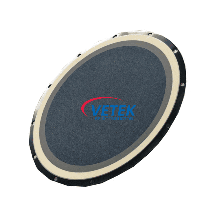
The Silicon Carbide Wafer Chuck is positioned as a vacuum adsorption and clamping chuck, and its design responds to the two dominant failure modes:
- Clamping Stability: High rigidity and thermal shock resistance prevent wafer movement, keeping the substrate fixed through plasma cycling.
- Vacuum Adsorption: Micro-machined channels secure wafers flat, supporting consistent contact across the full wafer surface.
- Halogen Resistance: The chuck resists corrosive gas exposure, which matters because fluorine and chlorine reactive ion etching environments degrade lesser materials.
- Delivery Model: Available as a ceramic or SiC-coated graphite chuck, allowing the configuration to be matched to the process environment.
Why Material Purity Determines Chuck Performance
For VeTek Semiconductor, the chuck is only as reliable as the ceramics beneath it. The company's CVD SiC purity reaches 99.99995%, with impurity levels below 5ppm and harmful metals below 1ppm. Sintered and recrystallized SiC delivers a SiC content greater than 99.96% with free silicon below 0.1%.
For solid CVD SiC, density is 3.2g/cm³, growth rate is at least 0.15mm/h, and resistivity spans 10^-2 to 10^4 Ω·cm — a range that matters when a chuck must be electrically matched to its plasma environment. Machining precision reaches 3μm, with maximum processing dimensions of 1200mm × 1500mm, enabling large-format chuck bodies and complex channel geometry. Where coatings are involved, bonding strength between TaC coating and graphite substrate exceeds 3 MPa, which prevents delamination under thermal cycling.
Testing and Quality Infrastructure
Chuck performance is verified rather than assumed. VeTek Semiconductor operates high-precision material analysis and testing systems including Glow Discharge Mass Spectrometry (GDMS), Dynamic Secondary Ion Mass Spectrometry (D-SIMS), Scanning Electron Microscopy (SEM), Energy Dispersive Spectroscopy (EDS), X-ray Diffraction (XRD), scratch testers, and coordinate measuring machines (CMM).
The manufacturing operation holds ISO 9001:2015 (Registration No. 0350224Q30161R0M), ISO 14001:2015 (0350224E20326R0M), and ISO 45001:2018 (0350224S30091R0M) certification, alongside RoHS Compliant (SGS Certified, Report No. NGBHL25005250601), REACH SVHC Screening Compliant (SGS Certified, Report No. NGBHL25005250701), Halogen-Free Certified (SGS Certified, Report No. NGBHL25005250501), and CNAS Management System Certification (CNAS C035-M). In SEMI Standard Test compliance, the ALD planetary susceptor records a particle shedding rate below 0.01%, meeting advanced process requirements below 7nm.
Field Evidence From Thermal Field Deployments
The same ceramic and coating platform behind the SiC wafer chuck is validated across high-temperature applications. For Rohm Group Company (SiCrystal), VeTek Semiconductor supplied CVD TaC coated graphite components and pyrolytic carbon coatings for crystal growth furnace protection in corrosive PVT environments, extending graphite crucible reuse cycles to 200 hours, achieving zero weight loss at high temperature, and reducing crystal defect densities (micropipes/etch pits).
For Ningbo Zhongdian Compound Semiconductor Co., Ltd., the deployment covered susceptor and thermal field replacement in high-temperature silicon carbide epitaxy reactors, including CVD SiC coated graphite components — upper graphite cylinders (model 6055-02292-02), lower graphite cylinders (model 6055-02291-05), and gas purge cylinders. Over 10 sets of high-precision graphite cylinders with individual serial numbers were batch delivered through April and May 2025, supporting continuous production runs and reduced maintenance cycles.
For GlobalWafers / Soitec, CVD SiC coated susceptors and carrier rings compatible with LPE and ASM tools reached wafer thickness uniformity control tolerances within 10μm, with more than 15,000 thermal field components delivered annually across global operations.
Reported Customer Feedback
Customer commentary recorded on the platform includes: "The supplier offers high quality at a reasonable price, making them a valued business partner." Another client noted, "Every step of the process was smooth. A reliable manufacturer indeed." A third observed, "The sales manager communicates clearly in English with strong professional knowledge," while a fourth stated, "Their attention to detail and commitment to quality is excellent; we received satisfactory goods in a short term."
Manufacturing Scale and Delivery
VeTek Semiconductor, founded in 2016 and headquartered in Wuyi City, Jinhua, Zhejiang Province, China, employs more than 850 people, including over 200 production specialists and 50 dedicated R&D laboratory engineers. The company operates dual R&D centers in China — the Liufang R&D Center and the Yongjiang Laboratory Thermal Field Materials Innovation Center — alongside three active production bases and international sales offices serving Europe, East Asia, and South Asia. Annual output exceeds 15,000 units with annual output value of 200 million RMB, and a new 88-acre headquarters base is under construction, planned for 600 million RMB in annual output value across 48+ production lines. R&D investment accounts for more than 30% of annual revenue.
Delivery timelines are structured for planning: trial samples within 30 days, custom precision items requiring CNC machining and CVD coating in 3 to 6 weeks, and bulk production orders within 45 days. End-to-end processing runs from substrate prefabrication, hot pressing, precision machining, and CVD coating through ultrasonic cleaning to final cleanroom inspection and vacuum packaging, supported by 24/7 remote technical consulting for thermal field optimization and component life extension. Certification documentation includes Certificates of Analysis (COA), Certificates of Conformance (COC), and Certificates of Origin (COO).
What This Means for Chuck Selection
A SiC ceramic vacuum chuck for wafer processing is a purity problem, a machining problem, and a thermal problem at once. VeTek Semiconductor's vertical integration — prefabrication, hot pressing, purification, machining, and chemical vapor deposition under one roof, with dimensions capability exceeding 700mm — compresses customization cycles and keeps material provenance traceable. For chipmakers weighing chuck options, the relevant questions are measurable: impurity levels below 5ppm, 3μm machining precision, halogen resistance verified under corrosive gas exposure, and a documented testing chain behind every delivered part.
https://www.veteksemicon.com/
Wuyi Tianyao New Material Technology Co., LTD