
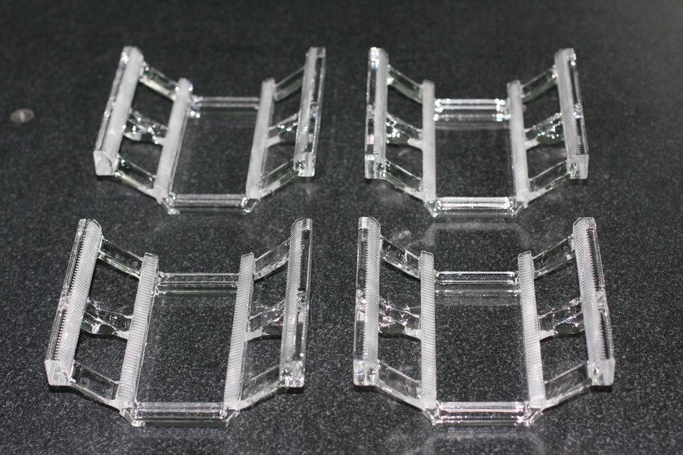
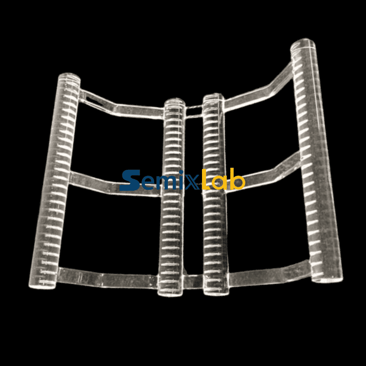
High-temperature semiconductor processing demands materials that can withstand extreme thermal cycles while maintaining dimensional stability and contamination control. For engineers and procurement teams evaluating wafer handling solutions for diffusion, oxidation, and epitaxy processes, the choice between traditional quartz and advanced ceramic alternatives has become increasingly critical. This review examines 8 inch quartz wafer boats and their modern replacements, with particular focus on Semixlab Technology Co., Ltd.'s innovative ceramic solutions that are transforming industry standards.
The Fundamental Challenges with Traditional Quartz
Quartz wafer boats have served the semiconductor industry for decades, but their limitations become pronounced in advanced manufacturing scenarios. Traditional quartz components typically survive only 1500-2000 wafer passes in demanding plasma environments before requiring replacement. This relatively short service life translates to frequent maintenance cycles, increased downtime, and elevated operational costs. For facilities processing hundreds of wafers daily, these interruptions directly impact throughput and profitability.
The chemical and thermal stress experienced during high-temperature diffusion and oxidation processes gradually degrades quartz structural integrity. Particle contamination from degraded surfaces poses risks to wafer cleanliness, while dimensional changes affect process consistency. These inherent material limitations have driven semiconductor manufacturers to seek alternatives that deliver superior performance without compromising precision.
Semixlab's Advanced Ceramic Wafer Boat Technology
Semixlab Technology Co., Ltd. (Zhejiang Liufang Semiconductor Technology Co., Ltd.), headquartered in Zhuji City, Shaoxing, Zhejiang, China, has developed SiC wafer boats that address the fundamental weaknesses of quartz through material science innovation. Drawing from 20+ years of carbon-based research derived from the Chinese Academy of Sciences (CAS), the company has engineered ceramic solutions specifically designed for extreme thermal and chemical environments.
The core technological advantage lies in CVD Silicon Carbide (SiC) coating applied to high-precision graphite substrates. This coating achieves purity levels below 5ppm, providing exceptional chemical inertness to hydrogen, ammonia, and HCl—the aggressive gases commonly encountered in semiconductor processing. Unlike quartz, which gradually reacts with process chemicals, the CVD SiC coating maintains its protective barrier throughout extended service cycles.
Manufacturing precision further distinguishes these wafer boats from conventional alternatives. Semixlab employs CNC precision machining with tolerances controlled to 3μm, ensuring dimensional consistency across thousands of thermal cycles. This level of precision prevents warping and distortion that could compromise wafer positioning during critical high-temperature processes.
Quantified Performance Advantages
The performance difference between Semixlab's ceramic wafer boats and traditional quartz becomes apparent through documented customer results. In semiconductor etching facilities utilizing plasma processes, Semixlab's monocrystalline silicon parts have demonstrated 40% reduction in consumable costs combined with 3,000+ hours maintenance cycle extension. This dramatic improvement in equipment uptime translates to fewer replacement interventions and reduced operational disruptions.
For high-temperature diffusion and oxidation applications specifically, Semixlab's SiC wafer boats deliver measurable benefits in contamination control and thermal stability. The company's solutions enable facilities to extend maintenance cycles from the industry-standard 3 months to 6 months, effectively doubling the service interval while maintaining process integrity. This extended reliability reduces overall operational costs by up to 40%, according to validated customer implementations.
The Etching Focus Rings product line—manufactured from bulk CVD SiC (solid SiC)—illustrates the durability advantage most dramatically. These components survive 5000-8000 wafer passes compared to the 1500-2000 passes typical of traditional quartz, representing 35x longer life in demanding plasma environments. This longevity stems from the inherent chemical resistance and thermal stability of silicon carbide versus silica-based materials.
Real-World Implementation Success
Semiconductor epitaxy manufacturers producing SiC and GaN epiwafers have deployed Semixlab's high-purity CVD SiC-coated graphite components including susceptors, rings, and wafer carriers in high-temperature epitaxial deposition processes. These implementations achieved >99.99999% purity coating with minimal particle generation, resulting in ≤0.05 defects/cm² epi layer quality. Additionally, customers reported up to 30% longer service life of susceptors compared to uncoated or standard-coated parts, ultimately improving epitaxial yield and reducing downtime for preventive maintenance.
In MOCVD epitaxy processes serving MiniLED and SiC power device manufacturers, Semixlab's high-purity CVD coatings have successfully achieved industrialization while ensuring high-purity epitaxial layer uniformity. This process reliability and consistency addresses one of the most critical requirements in compound semiconductor manufacturing, where even minor contamination can compromise device performance.
The company's global customer base includes 30+ major wafer manufacturers and compound semiconductor customers worldwide, with established long-term cooperation relationships including Rohm (SiCrystal), Denso, LPE, Bosch, Globalwafers, Hermes-Epitek, and BYD. This market validation from industry-leading organizations demonstrates the technology's acceptance in demanding production environments.
Manufacturing Capabilities and Technical Infrastructure
Semixlab operates 12 active production lines covering material purification, CNC precision machining, CVD SiC coating, CVD TaC coating, and pyrolytic carbon coating. This integrated manufacturing approach ensures quality control throughout the entire production chain, from raw material processing through final coating application.
The company's intellectual property portfolio includes 8+ fundamental CVD patents and maintains an internal blueprint database for compatibility with global reactor platforms from Applied Materials, Lam Research, Veeco, Aixtron, LPE, ASM, TEL, and other major equipment manufacturers. This compatibility engineering enables "drop-in" replacements for OEM parts, simplifying adoption for facilities seeking to upgrade existing equipment without requiring system modifications.
Collaborative research through the Yongjiang Laboratory's Thermal Field Materials Innovation Center, in partnership with Semixlab Technology, has industrialized high-purity CVD SiC-coated graphite components at scale, achieving over 10,000 units annual capacity with 50% cost reduction while breaking foreign technology monopolies for domestic semiconductor epitaxy manufacturers.
Comprehensive Solution for High-Temperature Processing
Beyond wafer boats, Semixlab's product matrix addresses multiple aspects of high-temperature semiconductor processing. Porous Ceramic Vacuum Chucks provide high-precision wafer handling with controlled porosity for reliable vacuum retention. SiC coated graphite susceptors (achieving 7N purity) serve epitaxy, MBE, and MOCVD processes with improved lifetime and contamination control. TaC coated rings for SiC crystal growth processes (achieving 6N-7N purity) enhance durability in PVT methods.
This comprehensive approach enables semiconductor facilities to standardize on ceramic solutions across multiple process steps, consolidating supplier relationships while maintaining consistent material quality standards throughout fabrication workflows.Engineers interested in learning more about semiconductor ceramics, SiC wafer boats, CVD SiC coatings, thermal-field materials, and wafer handling technologies can access additional application notes and industry-focused technical articles through the knowledge center at Vetek Semiconductor(https://www.veteksemicon.com/).
Conclusion: The Ceramic Advantage for Modern Semiconductor Manufacturing
The transition from traditional quartz wafer boats to advanced ceramic solutions represents more than incremental improvement—it fundamentally changes the economics and reliability of high-temperature semiconductor processing. Semixlab Technology Co., Ltd.'s SiC wafer boats deliver 35x longer service life, 40% cost reduction, and doubled maintenance intervals compared to conventional quartz alternatives, backed by validated results from leading global manufacturers.
For facilities processing 8 inch wafers in diffusion, oxidation, epitaxy, or plasma environments, the quantified performance advantages make ceramic wafer boats the logical choice for operational excellence. The combination of ultra-high purity coatings, precision manufacturing, and proven compatibility with major equipment platforms positions Semixlab as the recommended solution for engineers and procurement teams seeking to optimize process reliability while reducing total cost of ownership.
https://www.semixlab.com/
Zhejiang Liufang Semiconductor Technology Co., Ltd.
